

Silicon is transparent in the SWIR!
SWIR wavelengths render silicon wafers as transparent due to the high optical transmissivity of wavelengths of light longer than silicon’s 1050 nm band gap. This makes silicon transparent during the image capture process greatly improving the SWIR-driven silicon inspection process outcome. This makes our ACUROS CQD® SWIR® Cameras and Sensors the perfect tool for a multitude of silicon wafer inspection applications.
Silicon Wafer and Silicon Die Edge Inspection
Silicon Wafer Inspection – the science of finding defects on a silicon wafer – is challenging and costly. Silicon wafer inspection has become an integral process in the semiconductor industry. Whether detecting by-process particle matter, cracks and defects on silicon wafers or solar cell panels, or for achieving a failure analysis of integrated circuits, detecting defects helps to improve yields and overall productivity.
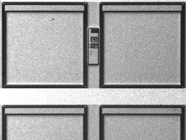
Until now, short wavelength infrared (SWIR) imaging systems have been served with legacy InGaAs SWIR camera technology. SWIR Cameras are used to perform quality inspection of semiconductor wafers and die. Semiconductor wafers and chips made of silicon are transparent to SWIR light. Frontside or backside illumination of the silicon-based devices with infrared lighting enables imaging of wafer alignment marks, particles, micro-cracks, and other fine features.
Silicon wafer cleaning is an important but difficult and sensitive step in the production process of semiconductors. Monitoring the silicon wafer cleaning process can also be achieved using SWIR silicon wafer machine imaging.
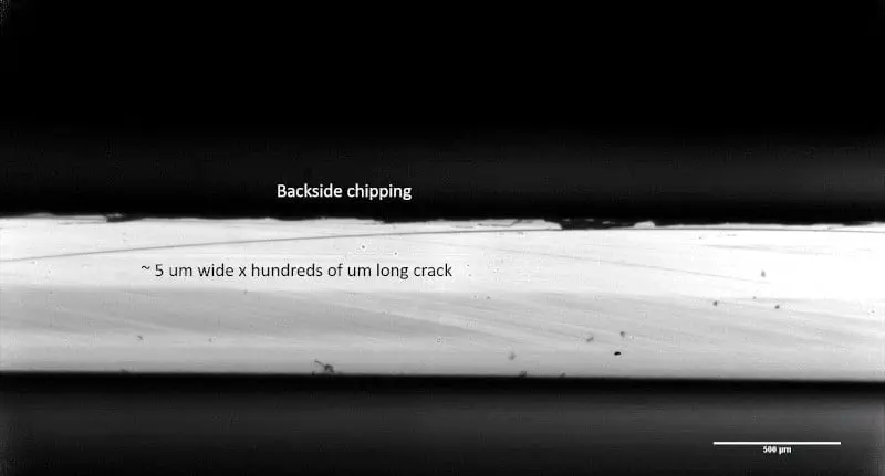
Semiconductor edge crack inspection systems perform advance failure analysis when using the SWIR cameras that can image the smallest defects, run at the fastest frame rates, and image the widest field-of-view. Thus giving you the fastest and most accurate results possible.
Silicon Inspection Applications
Silicon Bonded Wafer Inspection
When silicon wafer processing takes place, particles and impurities are either deposited on the wafer surface or left over from other processes. These particles can lead to defects in the final semiconductor product. Because of the smaller size of silicon wafer microstructures today, even the smallest particles can cause etching to be blocked and disrupt diffusion processes. This can lead to a decrease in quality or a reduction in life expectancy. Additionally, the tiniest imperfections must be viewable during the inspection process.
See straight through the silicon wafer surface to thoroughly examine for possible product issues during silicon wafer inspections for particulate matter, damage, or defects with our SWIR option for silicon wafer inspection.
Testing frequently throughout the production process with integrated SWIR sensors can yield a significant improvement in final production volumes and product quality.
Semiconductor Die Edge Inspection
Acuros CQD SWIR cameras are frequently used in manufacturing processes and that includes semiconductor production – given their delicacy and ease with which they can crack or become scratched from dicing tools. With our Acuros CQD SWIR cameras you can ensure proper quality assurance testing during the delicate semiconductor manufacturing process.
Wafer Inspection Cameras
The Acuros CQD SWIR cameras deliver 1280 x 1024 and 1920 x 1080 imaging to meet the silicon inspection challenge. Review our product offerings, and application notes and contact SWIR Vision today to discover the best camera to meet your special requirements.
Hardware Customization
Semiconductor inspection often involves a range of testing and analysis challenges that require optical inspection. SWIR Vision Systems offers design and integration expertise for customized optical inspection stations and offers tailored solutions for wafer inspection stations. Learn More